|
|
| Department of Electronics & Communication Engineering |
| |
| LABORATORY DETAILS |
| |
ADVANCED SIGNAL PROCESSING / ADVANCED VLSIDESIGN / ADVANCED COMPUTER NETWORKING LABORATORY |
| |
Technical Staff : Mr. N. Sathees Kumar |
| |
|
|
 |
 |
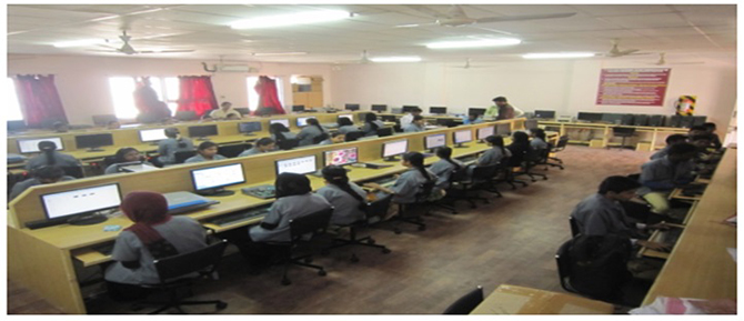
| Area of the laboratory: 13.37m ×9.14m =122.20 Sq. m |
|
| |
Description:
- Advanced Signal Processing Laboratory has been well furnished with25 KVA stabilizer and UPS
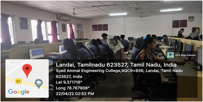
- There are 75 high configuration systems along with working tables facilitated in this laboratory
- Work tablesarehaving proper protecting devices such as fuse and MCB
- Each system is equipped with executedin ECE Computer Laboratory.
- This laboratory also covers embedded internet connection and IIR work bench for Embedded lab.
- Simulation experiments are system Lab, Computer Networks Lab,VLSI Design Lab, VLSI Laboratory I &VLSI Laboratory II courses prescribed by Anna University.
- Configuration Details: Dell Optiplex 390 DT–Nseries Base Intel core i3 2100 processor, Intel H-61chipset motherboard 2GB DDR-3RAM,320 GB SATA HDD,Dell Keyboard& optical mouse,Dell 18.5” TFT Monitor free DOS Pre loaded.
- Intel Core 2 Duo@2.93 GHz, Intel G41 Chipset Mother Board, 2GB DDR2@800 MHz RAM,320 GB@7200 rpm SATA HDD, Lenovo Keyboard, Lenovo Optical Mouse,Gigabit Ethernet Card, Micro Tower Cabinet, 18.5” TFT Color Monitor
- This lab having Six number of Analog Discovery kits.
- This lab consists of Licensed PSPICE, Xilinx, CADENCE and MATLAB.
- This lab has upgraded as Advanced VLSI laboratory under AICTE MODROBS in the Academic year 18-19.
|
| |
| Major Equipment’s Cost in Signal Processing Lab: Rs76,05,337 |
| |
| The following courses are conducted in this Laboratory. |
| |
| Sl. No |
Course Codes |
Lab Course Name |
Class |
| 1 |
VL4111 |
FPGA Laboratory |
I Sem M.E |
| 2 |
VL4112 |
Analog IC Design Laboratory |
I Sem M.E |
| 3 |
VL4211 |
Verification using UVM Laboratory |
II Sem M.E |
|
| |
| |
|
|


